Early access to emerging technologies and strong connections to worldwide centres of academic and industrial excellence, have kept Sivers Photonics at the forefront of the III-V compound semiconductor market for almost 20 years.
Sivers Photonics partners with leading worldwide academic and corporate institutions to continuously grow its design, development, manufacture and process engineering IP portfolio.
We are involved in joint research projects with many universities and have collaborations in place with industry research and innovation centres, such as IMEC. We are an active partner in many UK and European, Technology Consortium Programmes, with members ranging from start-up companies to global corporations.
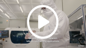 Collaborating with IMEC and ASMPT since 2019, significant progress has been made in the successful hybrid integration of DFB laser onto silicon photonics integrated circuits.Reference interface designs and assembly processes have been created for flip-chip bonding DFB lasers from Sivers’ InP 100 product platform, with sub 0.5-μm precision, enabling reproducible coupling losses below 2dB and waveguide-coupled power as high as 40mW.
This integration of DFB lasers into silicon photonic integrated circuits allows for the creation of compact, low-power, and cost-effective devices that can operate at high speeds over long distances and can target a a broad range of applications, including optical communications, optical 3D sensing (LiDAR), biophotonics, high-precision metrology, gas sensing and more.
Watch the video and find our more about the collaboration.
LEARN MORE ABOUT the COLLABORATION
Today’s high volume datacom optics defined by IEEE and MSA standards specify serial or four WDM interfaces. The CW-WDM MSA (Continuous-Wave Wavelength Division Multiplexing Multi-Source Agreement) was formed to standardize WDM CW sources in O-band for emerging advanced integrated optics applications that are expected to move to 8, 16, and 32 wavelengths. Such higher wavelength counts are needed for emerging applications such as AI, HPC, and high-density optics, and enable a leap in performance, efficiency, cost, and bandwidth scaling compared with other technologies. The new specifications will leverage IEEE and ITU-T standards.
There is no plan to standardize link parameters as these will remain unique to applications. Standardization of mechanical form factors will not be part of the first MSA standard but will be considered in follow-on specs.
The CW-WDM MSA is enabling Sivers Photonics to provide next generation DFB lasers in a more standard format, to customers including Ayar Labs. This will eliminate the high levels of complex customization we often see today.
For further information visit the CW-WDM MSA website and read our latest Insight Paper, “CW-WDM MSA Compliant InP Laser Sources for Hybrid Silicon Photonic Integration”
Sivers Photonics are key to the commercialisation of quantum technology, collaborating with academia, industry and government across several ground-breaking projects shaping the quantum landscape. Our technology will enable critical real-world applications in areas such as LIDAR, consumer technology and data communications.

Driver Assisted and Autonomous Vehicles
Sivers are part of a government led quantum collaboration project, SPIDAR, developing range finding and 3D imaging systems for driver assisted and autonomous vehicles. The project, collaboration with high-profile commercial partners Toshiba, Network Rail and Thales UK, amongst others.
The SPIDAR project will develop single-photon, infrared imaging, detection and ranging technology, used to sense the proximity of objects and other vehicles for driver safety and self-driving vehicle applications. Cameras are used to detect single photon light particles in the infrared region of the electromagnetic spectrum. The distance to the detected object or range is the measured time from the photon’s emission to the object and back again. The photon detector delivers sub-nanosecond precision, detecting single photons from the faintest possible reflections. This technology enables a far greater detection range for 3D cameras than is currently available, enhancing both safety and effectiveness when deployed in real-life applications like vehicle safety. The market is valued at $556bn by 2026*
* ‘Global Autonomous Vehicle Market’ from Allied Market Research

The world’s first commercial Quantum Atomic Magnetometer
Sivers are working as part of the MAG-V project aimed at developing the world’s first, commercial Quantum Atomic Magnetometer, to detect micro-defects in ferrous metal surfaces that are not usually visible to the human eye and can be hidden underground or behind protective or insulating coatings. These quantum magnetometers are developed for non-intrusive corrosion detection, which is a billion-dollar market.

Atomic Clocks
We’re also working to develop Quantum Gallium Nitride (Q-GaN) visible light laser diode sources, suitable for quantum sensing and specialised telecommunications applications. The prime Q-GaN laser technology application is in atomic clocks, helping to ensure accurate GPS coverage when satellite connections are weak or lost. Transport industries will benefit first, with the technology expected to be miniaturised for smartphones and smartwatches, opening up a wide range of consumer applications in the future. The project is funded by the European R&D initiative Eurostars working in collaboration with project partner, TopGaN Ltd Poland.
For more information about Sivers Photonics, or to discuss your Photonics project requirements.